FET Principles And Circuits — Part 1
By Ray Marston
FET (Field-Effect Transistor) Basics
Field-Effect Transistors (FETs) are unipolar devices, and have two big advantages over bipolar transistors: one is that they have a near-infinite input resistance and thus offer near-infinite current and power gain; the other is that their switching action is not marred by charge-storage problems, and they thus outperform most bipolars in terms of digital switching speeds.
Several different basic types of FETs are available, and this opening episode looks at their basic operating principles. Parts 2 to 4 of the series will show practical ways of using FETs.
FET BASICS
 |
|
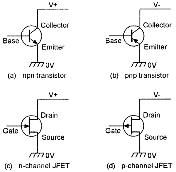
FIGURE 1. Comparison of transistor and JFET symbols, notations, and supply polarities. |
An FET is a three-terminal amplifying device. Its terminals are known as the source, gate, and drain, and correspond respectively to the emitter, base, and collector of a normal transistor. Two distinct families of FETs are in general use. The first of these is known as ‘junction-gate’ types of FETs; this term generally being abbreviated to either JUGFET or (more usually) JFET.The second family is known as either ‘insulated-gate’ FETs or Metal Oxide Semiconductor FETs, and these terms are generally abbreviated to IGFET or MOSFET, respectively. ‘N-channel’ and ‘p-channel’ versions of both types of FET are available, just as normal transistors are available in npn and pnp versions. Figure 1 shows the symbols and supply polarities of both types of bipolar transistor, and compares them with both JFET versions.
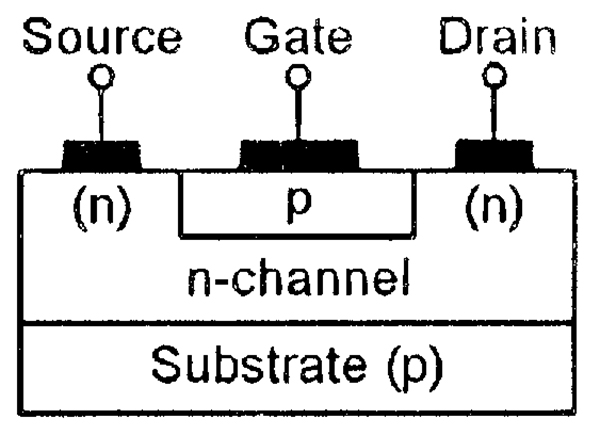
Figure 2 illustrates the basic construction and operating principles of a simple n-channel JFET. It consists of a bar of n-type semiconductor material with a drain terminal at one end and a source terminal at the other. A p-type control electrode or gate surrounds (and is joined to the surface of) the middle section of the n-type bar, thus forming a p-n junction.
 |
|
FIGURE 2. Basic structure of a simple n-channel JFET, showing how channel width is controlled via the gate bias. |
In normal use, the drain terminal is connected to a positive supply and the gate is biased at a value that is negative (or equal) to the source voltage, thus reverse-biasing the JFET’s internal p-n junction, and accounting for its very high input impedance.
With zero gate bias applied, a current flow from drain to source via a conductive ‘channel’ in the n-type bar is formed. When negative gate bias is applied, a high resistance region is formed within the junction, and reduces the width of the n-type conduction channel and thus reduces the magnitude of the drain-to-source current. As the gate bias is increased, the ‘depletion’ region spreads deeper into the n-type channel, until eventually, at some ‘pinch-off’ voltage value, the depletion layer becomes so deep that conduction ceases.
Thus, the basic JFET of Figure 2 passes maximum current when its gate bias is zero, and its current is reduced or ‘depleted’ when the gate bias is increased. It is thus known as a ‘depletion-type’ n-channel JFET. A p-channel version of the device can (in principle) be made by simply transposing the p and n materials.
JFET DETAILS
 |
|
FIGURE 3. Construction of n-channel JFET. |
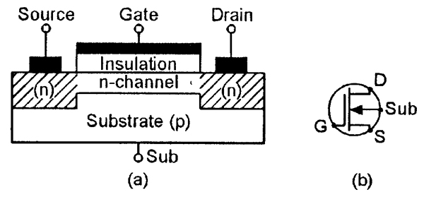
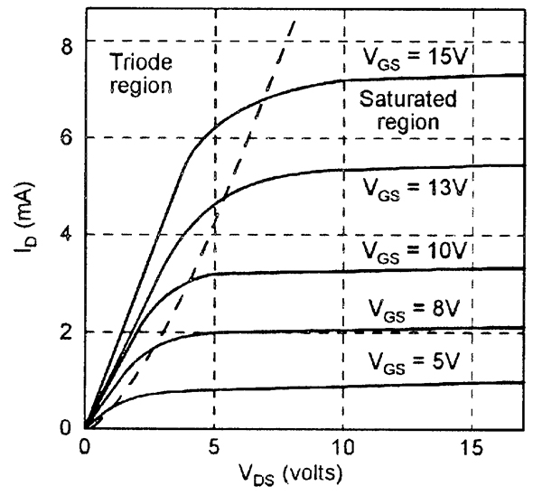
Figure 3 shows the basic form of construction of a practical n-channel JFET; a p-channel JFET can be made by transposing the p and n materials. All JFETs operate in the depletion mode, as already described. Figure 4 shows the typical transfer characteristics of a low-power n-channel JFET, and illustrates some important features of this type of device. The most important characteristics of the JFET are as follows:
(1) When a JFET is connected to a supply with the polarity shown in Figure 1 (drain +ve for an n-channel FET, -ve for a p-channel FET), a drain current (ID) flows and can be controlled via a gate-to-source bias voltage VGS.
 |
|
FIGURE 4. Idealized transfer characteristics of an n-channel JFET. |
(2) ID is greatest when VGS = 0, and is reduced by applying a reverse bias to the gate (negative bias in an n-channel device, positive bias in a p-type). The magnitude of VGS needed to reduce ID to zero is called the ‘pinch-off’ voltage, VP, and typically has a value between 2 and 10 volts. The magnitude of ID when VGS = 0 is denoted IDSS, and typically has a value in the range 2 to 20mA.
(3) The JFET’s gate-to-source junction has the characteristics of a silicon diode. When reverse-biased, gate leakage currents (IGSS) are only a couple of nA (1nA = .001µA) at room temperature. Actual gate signal currents are only a fraction of an nA, and the input impedance of the gate is typically thousands of megohms at low frequencies. The gate junction is shunted by a few pF, so the input impedance falls as frequency rises.
If the JFET’s gate-to-source junction is forward-biased, it conducts like a normal silicon diode. If it is excessively reverse-biased, it avalanches like a zener diode. In either case, the JFET suffers no damage if gate currents are limited to a few mA.
 |
|
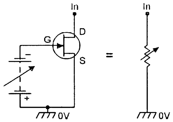
FIGURE 5. An n-channel JFET can be used as a voltage-controlled resistor. |
 |
|
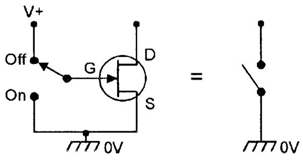
FIGURE 6. An n-channel JFET can be used as a voltage-controlled switch. |
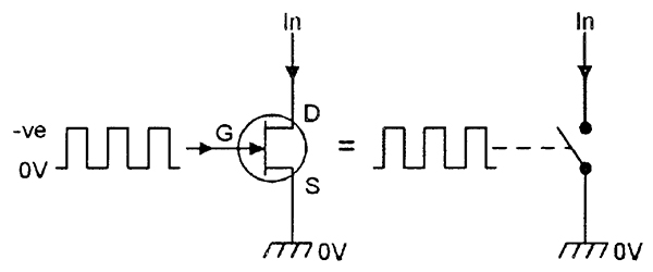
(4) Note in Figure 4 that, for each VGS value, drain current ID rises linearly from zero as the drain-to-source voltage (VDS) is increased from zero up to some value at which a ‘knee’ occurs on each curve, and that ID then remains virtually constant as VDS is increased beyond the knee value. Thus, when VDS is below the JFET’s knee value, the drain-to-source terminals act as a resistor, RDS, with a value dictated by VGS, and can thus be used as a voltage-variable resistor, as in Figure 5.
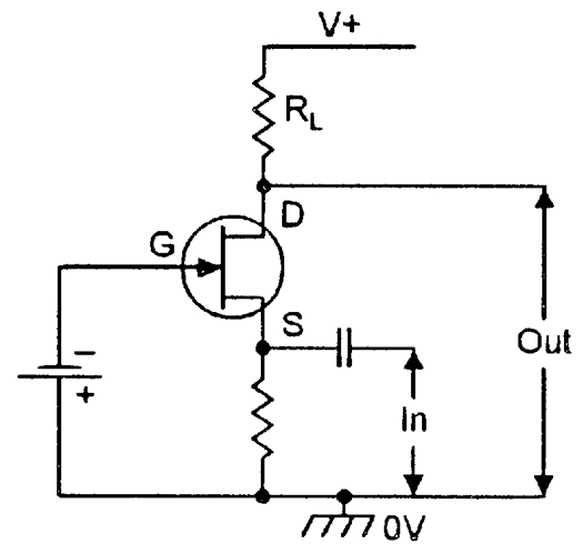
Typically, RDS can be varied from a few hundred ohms (at VGS = 0) to thousands of megohms (at VGS = VP), enabling the JFET to be used as a voltage-controlled switch (Figure 6) or as an efficient ‘chopper’ (Figure 7) that does not suffer from offset-voltage or saturation-voltage problems.
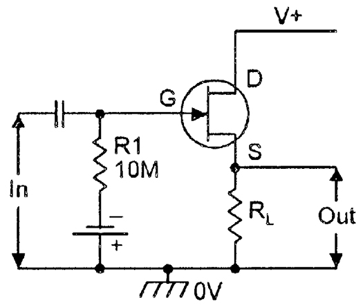
Also note in Figure 4 that when VDS is above the knee value, the ID value is controlled by the VGS value and is almost independent of VDS, i.e., the JFET acts as a voltage-controlled current generator. The JFET can be used as a fixed-value current generator by either tying the gate to the source as in Figure 8(a), or by applying a fixed negative bias to the gate as in Figure 8(b). Alternatively, it can (when suitably biased) be used as a voltage-to-current signal amplifier.
 |
 |
|
FIGURE 7. An n-channel JFET can be used as an electronic chopper. |
FIGURE 8. An n-channel JFET can be used as a constant-current generator. |
(5) FET ‘gain’ is specified as transconductance, gm, and denotes the magnitude of change of drain current with gate voltage, i.e., a gm of 5mA/V signifies that a VGS variation of one volt produces a 5mA change in ID. Note that the form I/V is the inverse of the ohms formula, so gm measurements are often expressed in ‘mho’ units. Usually, gm is specified in FET data sheets in terms of mmhos (milli-mhos) or µmhos (micro-mhos). Thus, a gm of 5mA/V = 5-mmho or 5000-µmho.
 |
|
FIGURE 9. Basic n-channel common-source amplifier JFET circuit. |
 |
|
FIGURE 10. Basic n-channel common-drain (source-follower) JFET circuit. |
 |
|
FIGURE 11. Basic n-channel common-gate JFET circuit. |
In most practical applications, the JFET is biased into the linear region and used as a voltage amplifier. Looking at the n-channel JFET, it can be used as a common source amplifier (corresponding to the bipolar npn common emitter amplifier) by using the basic connections in Figure 9.
Alternatively, the common drain or source follower (similar to the bipolar emitter follower) configuration can be obtained by using the connections in Figure 10, or the common gate (similar to common base) configuration can be obtained by using the basic Figure 11 circuit. In practice, fairly accurate biasing techniques (discussed in Part 2 of this series) must be used in these circuits.
THE IGFET/MOSFET
The second (and most important) family of FETs are those known under the general title of IGFET or MOSFET. In these FETs, the gate terminal is insulated from the semiconductor body by a very thin layer of silicon dioxide, hence the title ‘Insulated Gate Field Effect Transistor,’ or IGFET. Also, the devices generally use a ‘Metal-Oxide Silicon’ semiconductor material in their construction, hence the alternative title of MOSFET.
Figure 12 shows the basic construction and the standard symbol of the n-channel depletion-mode FET. It resembles the JFET, except that its gate is fully insulated from the body of the FET (as indicated by the Figure 12(b) symbol) but, in fact, operates on a slightly different principle to the JFET.
It has a normally-open n-type channel between drain and source, but the channel width is controlled by the electrostatic field of the gate bias. The channel can be closed by applying suitable negative bias, or can be increased by applying positive bias.
In practice, the FET substrate may be externally available, making a four-terminal device, or may be internally connected to the source, making a three-terminal device.
An important point about the IGFET/MOSFET is that it is also available as an enhancement-mode device, in which its conduction channel is normally closed but can be opened by applying forward bias to its gate.
Figure 13 shows the basic construction and the symbol of the n-channel version of such a device. Here, no n-channel drain-to-source conduction path exists through the p-type substrate, so with zero gate bias there is no conduction between drain and source; this feature is indicated in the symbol of Figure 13(b) by the gaps between source and drain.
 |
 |
|
FIGURE 12. Construction (a) and symbol (b) of n-channel depletion-mode IGFET/MOSFET. |
FIGURE 13. Construction (a) and symbol (b) of n-channel enhancement-mode IGFET/MOSFET. |
To turn the device on, significant positive gate bias is needed, and when this is of sufficient magnitude, it starts to convert the p-type substrate material under the gate into an n-channel, enabling conduction to take place.
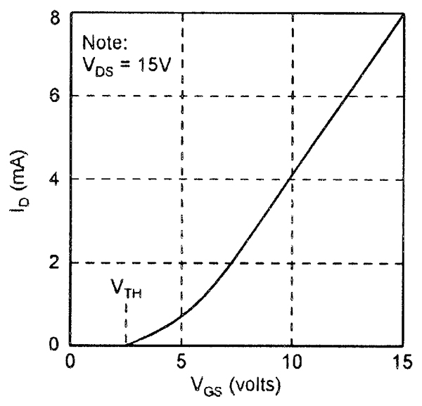
Figure 14 shows the typical transfer characteristics of an n-channel enhancement-mode IGFET/MOSFET, and Figure 15 shows the VGS/ID curves of the same device when powered from a 15V supply. Note that no ID current flows until the gate voltage reaches a ‘threshold’ (VTH) value of a few volts, but that beyond this value, the drain current rises in a non-linear fashion.
 |
 |
|
FIGURE 14. Typical transfer characteristics of n-channel enhancement-mode IGFET/MOSFET. |
FIGURE 15. Typical VGS/ID characteristics of n-channel enhancement-mode IGFET/MOSFET |
Also note that the transfer graph is divided into two characteristic regions, as indicated (in Figure 14) by the dotted line, these being the ‘triode’ region and the ‘saturated’ region. In the triode region, the device acts like a voltage-controlled resistor; in the saturated region, it acts like a voltage-controlled constant-current generator.
 |
|
Figure 16. Internally-protected n-channel depletion-mode IGFET/MOSFET. |
The basic n-channel MOSFETs of Figures 12 and 13 can — in principle — be converted to p-channel devices by simply transposing their p and n materials, in which case their symbols must be changed by reversing the directions of their substrate arrows.
A number of sub-variants of the MOSFET are in common use. The type known as ‘DMOS’ uses a double-diffused manufacturing technique to provide it with a very short conduction channel and a consequent ability to operate at very high switching speeds. Several other MOSFET variants are described in the remainder of this opening episode.
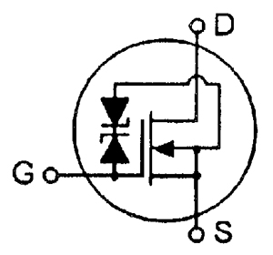
Note that the very high gate impedance of MOSFET devices makes them liable to damage from electrostatic discharges and, for this reason, they are often provided with internal protection via integral diodes or zeners, as shown in the example in Figure 16.
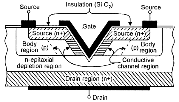
VFET DEVICES
In a normal small-signal JFET or MOSFET, the main signal current flows ‘laterally’ (see Figures 3, 12, and 13) through the device’s conductive channel. This channel is very thin, and maximum operating currents are consequently very limited (typically to maximum values in the range 2 to 40mA).
In post-1970 times, many manufacturers have tried to produce viable high-power/high-current versions of the FET, and the most successful of these have relied on the use of a ‘vertical’ (rather than lateral) flow of current through the conductive channel of the device. One of the best known of these devices is the ‘VFET,’ an enhancement-mode power MOSFET which was first introduced by Siliconix way back in 1976.
 |
|
FIGURE 17. Basic structure of the VFET power device. |
Figure 17 shows the basic structure of the original Siliconix VFET. It has an essentially four-layer structure, with an n-type source layer at the top, followed by a p-type ‘body’ layer, an epitaxial n-type layer, and (at the bottom) an n-type drain layer. Note that a ‘V’ groove (hence the ‘VFET’ title) passes through the first two layers and into the third layer of the device, and is electrostatically connected (via an insulating silicon dioxide film) to the gate terminal.
If the gate is shorted to the source, and the drain is made positive, no drain-to-source current flows, because the diode formed by the p and n materials is reverse-biased. But if the gate is made positive to the source, the resulting electrostatic field converts the area of p-type material adjacent to the gate into n-type material, thus creating a conduction channel in the position shown in Figure 17 and enabling current to flow vertically from the drain to the source.
As the gate becomes more positive, the channel width increases, enabling the drain-to-source current to increase as the drain-to-source resistance decreases. This basic VFET can thus pass reasonably high currents (typically up to 2A) without creating excessive current density within the channel regions.
The original Siliconix VFET design of Figure 17 was successful, but imperfect. The sharp bottom of its V-groove caused an excessive electric field at this point and restricted the device’s operating voltage. Subsequent to the original VFET introduction, Intersil introduced their own version of the ‘VMOS’ technique, with a U-shaped groove (plus other modifications) that improved device reliability and gave higher maximum operating currents and voltages. In 1980, Siliconix added these and other modifications to their own VFET devices, resulting in further improvements in performance.
OTHER POWER FETs
Several manufacturers have produced viable power FETs without using ‘V’- or ‘U’-groove techniques, but still relying on the vertical flow of current between drain and source. In the 1980s, Hitachi produced both p-channel and n-channel power MOSFET devices with ratings up to 8A and 200V; these devices were intended for use mainly in audio and low-RF applications.
Supertex of California and Farranti of England pioneered the development of a range of power MOSFETS with the general title of ‘vertical DMOS.’ These featured high operating voltages (up to 650V), high current rating (up to 16A), low on resistance (down to 50 milliohms), and very fast operating speeds (up to 2GHz at 1A, 500MHz at 10A).
Siemens of West Germany used a modified version of DMOS, known as SIPMOS, to produce a range of n-channel devices with voltage ratings as high as 1kV and with current ratings as high as 30A.
 |
|
FIGURE 18. The IR HEXFET comprises a balanced matrix of parallel-connected low-power MOSFETs, which are equivalent to a single high-power MOSFET. |
One International Rectifier solution to the power MOSFET problem is a device which, in effect, houses a vast array of parallel-connected low-power vertical MOSFETs or ‘cells’ which share the total current equally between them, and thus act like a single high-power MOSFET, as indicated in Figure 18. These devices are named HEXFET, after the hexagonal structure of these cells, which have a density of about 100,000 per square centimeter of semiconductor material.
Several manufacturers produce power MOSFETs that each comprise a large array of parallel-connected low-power lateral (rather than horizontal) MOSFET cells that share the total operating current equally between them; the device thus acts like a single high-power MOSFET. These high-power devices are known as lateral MOSFETs or L-MOSFETs, and give a performance that is particularly useful in super-fi audio power amplifier applications.
Note that, in parallel-connected MOSFETs (as used in the internal structure of the HEXFET and L-MOSFET devices described above), equal current sharing is ensured by the conduction channel’s positive temperature coefficient; if the current in one MOSFET becomes excessive, the resultant heating of its channel raises its resistance, thus reducing its current flow and tending to equalize it with that of other parallel-connected MOSFETs. This feature makes such power MOSFETs almost immune to thermal runaway problems.
Today, a vast range of power MOSFET types are manufactured. ‘Low voltage’ n-channel types are readily available with voltage/current ratings as high as 100V/75A, and ‘high voltage’ ones with ratings as high as 500V/25A.
 |
|
FIGURE 19. The basic internal circuitry (a) and the circuit symbol (b) of the TOPFET (Temperature and Overload Protected MOSFET). |
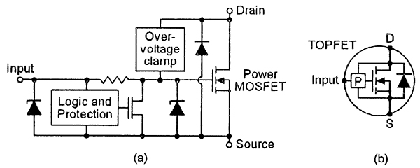
One of the most important recent developments in the power-MOSFET field has been the introduction of a variety of so-called ‘intelligent’ or ‘smart’ MOSFETs with built-in overload protection circuitry; these MOSFETs usually carry a distinctive registered trade name. Philips devices of this type are known as TOPFETs (Temperature and Overload Protected MOSFETs); Figure 19 shows (in simplified form) the basic internal circuitry and the circuit symbol of the TOPFET.
The Siemens version of the smart MOSFET is known as the PROFET. PROFET devices incorporate protection against damage from short circuits, over temperature, overload, and electrostatic discharge (ESD). International Rectifier produce a range of smart n-channel MOSFET known as SMARTFETs; these incorporate protection against damage from short circuits, over temperature, overvoltage, and ESD.
 |
|
FIGURE 20. Normal circuit symbol of the IGBT (Insulated Gate Bipolar Transistor). |
Finally, yet another recent and important development in the n-channel power MOSFET field, has been the production — by various manufacturers — of a range of high power devices known as IGBTs (Insulated Gate Bipolar Transistors), which have a MOSFET-type input and an internally protected high-voltage high-current bipolar transistor output. Figure 20 shows the normal circuit symbol of the IGBT. Devices of this type usually have voltage/current/power ratings ranging from as low as 600V/6A/33W (in the device known as the HGTD3N603), to as high as 1200V/520A/3000W (in the device known as the MG400Q1US51).
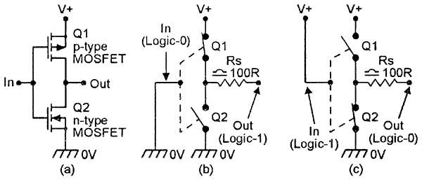
CMOS BASICS
One major FET application is in digital ICs. The best known range of such devices use the technology known as CMOS, and rely on the use of complementary pairs of MOSFETs. Figure 21 illustrates basic CMOS principles. The basic CMOS device comprises a p-type and n-type pair of enhancement-mode MOSFETs, wired in series, with their gates shorted together at the input and their drains tied together at the output, as shown in Figure 21(a). The pair are meant to use logic-0 or logic-1 digital input signals, and Figures 21(b) and 21(c), respectively, show the device’s equivalent circuit under these conditions.
 |
|
FIGURE 21. Basic CMOS circuit (a), and its equivalent with (b) a logic-0 input and (c) a logic-1 input. |
When the input is at logic-0, the upper (p-type) MOSFET is biased fully on and acts like a closed switch, and the lower (n-type) MOSFET is biased off and acts like an open switch; the output is thus effectively connected to the positive supply line (logic-1) via a series resistance of about 100R.
When the input is at logic-1, the MOSFET states are reversed, with Q1 acting like an open switch and Q2 acting like a closed switch, so the output is effectively connected to ground (logic-0) via 100R. Note in both cases that the entire signal current is fed to the load, and none is shunted off by the CMOS circuitry; this is a major feature of CMOS technology. NV