Practical JFET circuits.
Last month’s opening episode explained (among other things) the basic operating principles of JFETs. JFETs are low-power devices with a very high input resistance and invariably operate in the depletion mode, i.e., they pass maximum current when the gate bias is zero, and the current is reduced (‘depleted’) by reverse-biasing the gate terminal.
 |
||
|
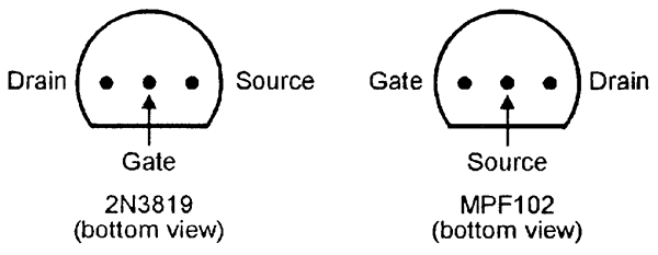
FIGURE 1. Outline and connections of the 2N3819 and MPF102
JFETs. |
||
| Parameter | 2N3918 | MPF102 |
| VDS max (= max. drain-to-source voltage) | 25V | 25V |
| VDG max (= max. drain-to-gate voltage) | 25V | 25V |
| VGS max (= max. gate-to-source voltage) | 25V | 25V |
| IDSS (= drain-to-source current with VGS = 0V) | 2-20mA | 2-20mA |
| IGSS max (= gate leakage current at 25° C) | 2nA | 2nA |
| PT max (= max. power dissipation, in free air) | 200mW | 310mW |
| Figure 2. Basic characteristics of the 2N3819 and MPF102 n-channel JFETs. | ||
Most JFETs are n-channel (rather than p-channel) devices. Two of the oldest and best known n-channel JFETs are the 2N3819 and the MPF102, which are usually housed in TO92 plastic packages with the connections shown in Figure 1; Figure 2 lists the basic characteristics of these two devices.
This month’s article looks at basic usage information and applications of JFETs. All practical circuits shown here are specifically designed around the 2N3819, but will operate equally well when using the MPF102.
JFET BIASING
The JFET can be used as a linear amplifier by reverse-biasing its gate relative to its source terminal, thus driving it into the linear region. Three basic JFET biasing techniques are in common use. The simplest of these is the ‘self-biasing’ system shown in Figure 3, in which the gate is grounded via Rg, and any current flowing in Rs drives the source positive relative to the gate, thus generating reverse bias.
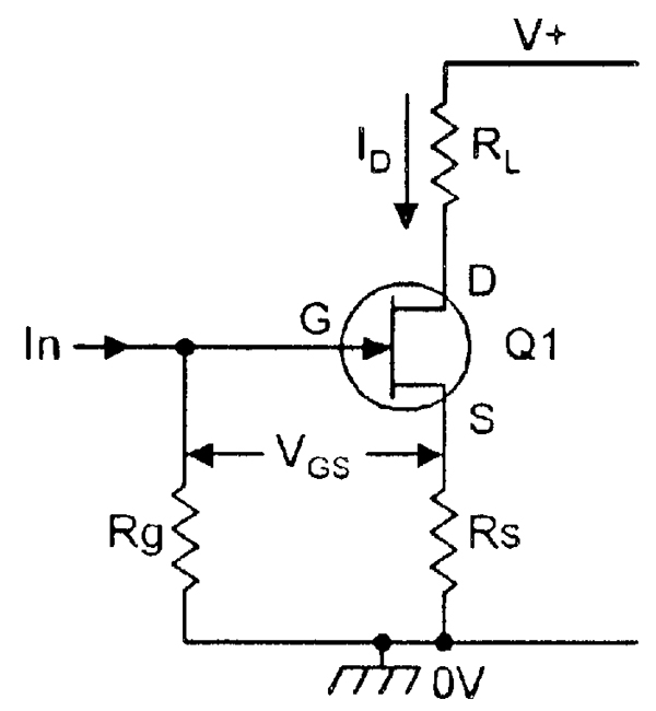 |
| FIGURE 3. Basic JFET ‘self-biasing’ system. |
Suppose that an ID of 1mA is wanted, and that a VGS bias of -2V2 is needed to set this condition; the correct bias can obviously be obtained by giving Rs a value of 2k2; if ID tends to fall for some reason, VGS naturally falls as well, and thus makes ID increase and counter the original change; the bias is thus self-regulating via negative feedback.
In practice, the VGS value needed to set a given ID varies widely between individual JFETS, and the only sure way of getting a precise ID value in this system is to make Rs a variable resistor; the system is, however, accurate enough for many applications, and is the most widely used of the three biasing methods.
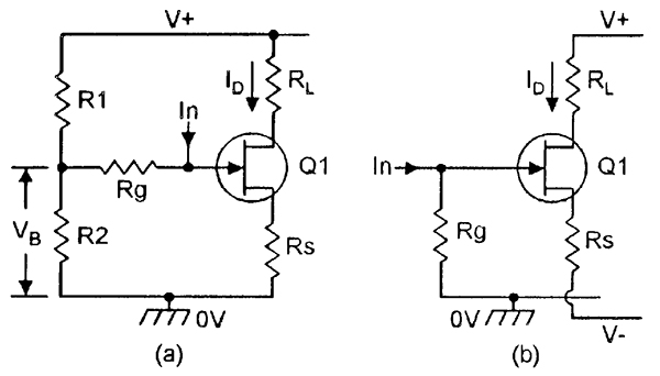 |
| FIGURE 4. Basic JFET ‘offset-biasing’ system. |
A more accurate way of biasing the JFET is via the ‘offset’ system of Figure 4(a), in which divider R1-R2 applies a fixed positive bias to the gate via Rg, and the source voltage equals this voltage minus VGS. If the gate voltage is large relative to VGS, ID is set mainly by Rs and is not greatly influenced by VGS variations. This system thus enables ID values to be set with good accuracy and without need for individual component selection. Similar results can be obtained by grounding the gate and taking the bottom of Rs to a large negative voltage, as in Figure 4(b).
The third type of biasing system is shown in Figure 5, in which constant-current generator Q2 sets the ID, irrespective of the JFET characteristics. This system gives excellent biasing stability, but at the expense of increased circuit complexity and cost.
In the three biasing systems described, Rg can have any value up to 10M, the top limit being imposed by the volt drop across Rg caused by gate leakage currents, which may upset the gate bias.
 |
 |
 |
| FIGURE
5. Basic JFET ‘constant-current’ biasing system. |
FIGURE 6. Self-biasing source follower. Zin = 10M. | FIGURE 7. Source follower with offset biasing. Zin = 44M. |
SOURCE FOLLOWER CIRCUITS
When used as linear amplifiers, JFETs are usually used in either the source follower (common drain) or common-source modes. The source follower gives a very high input impedance and near-unity voltage gain (hence the alternative title of ‘voltage follower’).
Figure 6 shows a simple self-biasing (via RV1) source follower; RV1 is used to set a quiescent R2 volt-drop of 5V6. The circuit’s actual input-to-output voltage gain is 0.95. A degree of bootstrapping is applied to R3 and increases its effective impedance; the circuit’s actual input impedance is 10M shunted by 10pF, i.e., it is 10M at very low frequencies, falling to 1M0 at about 16kHz and 100k at 160kHz, etc.
Figure 7 shows a source follower with offset gate biasing. Overall voltage gain is about 0.95. C2 is a bootstrapping capacitor and raises the input impedance to 44M, shunted by 10pF.
 |
| FIGURE 8. Hybrid source follower. Zin = 500M. |
Figure 8 shows a hybrid (JFET plus bipolar) source follower. Offset biasing is applied via R1-R2, and constant-current generator Q2 acts as a very high-impedance source load, giving the circuit an overall voltage gain of 0.99. C2 bootstraps R3’s effective impedance up to 1000M, which is shunted by the JFET’s gate impedance; the input impedance of the complete circuit is 500M, shunted by 10pF.
Note then if the high effective value of input impedance of this circuit is to be maintained, the output must either be taken to external loads via an additional emitter follower stage (as shown dotted in the diagram) or must be taken only to fairly high impedance loads.
COMMON SOURCE AMPLIFIERS
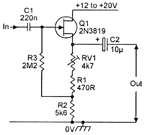
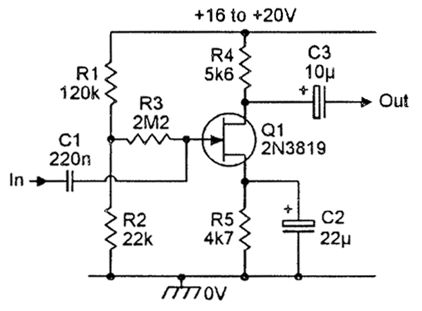
Figure 9 shows a simple self-biasing common source amplifier; RV1 is used to set a quiescent 5V6 across R3. The RV1-R2 biasing network is AC-decoupled via C2, and the circuit gives a voltage gain of 21dB (= x12), and has a ±3dB frequency response that spans 15Hz to 250kHz and an input impedance of 2M2 shunted by 50pF. (This high shunt value is due to Miller feedback, which multiplies the JFET’s effective gate-to-drain capacitance by the circuit’s x12 Av value.)
 |
 |
| FIGURE 9. Simple self-biasing common-source amplifier. | FIGURE 10. Simple headphone amplifier. |
Figure 10 shows a simple self-biasing headphone amplifier
that can be used with headphone impedances of 1k0 or greater. It has a
built-in volume control (RV1), has an input impedance of 2M2, and can use
any supply in the 9V to 18V range.
 |
 |
| FIGURE 11. General-purpose add-on pre-amplifier. | FIGURE
12. Common-source amplifier with offset gate biasing. |
 |
| FIGURE 13. ‘Hybrid’ common-source amplifier. |
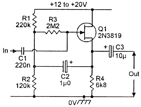
Figure 11 shows a self-biasing add-on pre-amplifier that gives a voltage gain in excess of 20dB, has a bandwidth that extends beyond 100kHz, and has an input impedance of 2M2. It can be used with any amplifier that can provide a 9V to 18V power source.
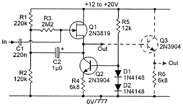
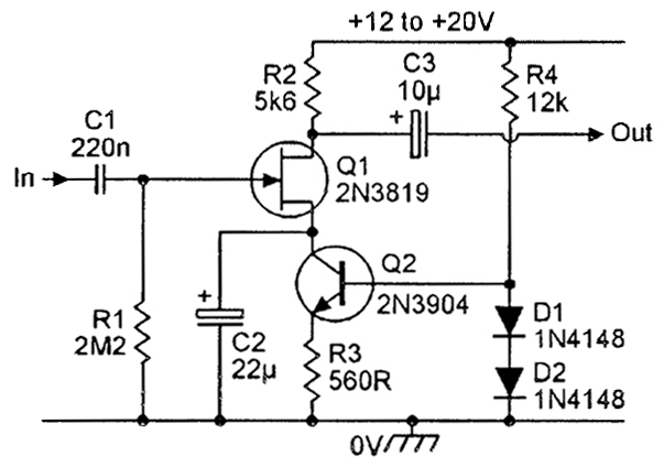
JFET common source amplifiers can — when very high biasing accuracy is needed — be designed using either the ‘offset’ or ‘constant-current’ biasing technique. Figures 12 and 13 show circuits of these types. Note that the ‘offset’ circuit of Figure 12 can be used with supplies in the range 16V to 20V only, while the hybrid circuit of Figure 13 can be used with any supply in the 12V to 20V range. Both circuits give a voltage gain of 21dB, a ±3dB bandwidth of 15Hz to 250kHz, and an input impedance of 2M2.
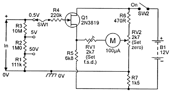
DC VOLTMETERS
Figure 14 shows a JFET used to make a very simple and basic three-range DC voltmeter with a maximum FSD sensitivity of 0.5V and an input impedance of 11M1. Here, R6-RV2 and R7 form a potential divider across the 12V supply and — if the R7-RV2 junction is used as the circuit’s zero-voltage point — sets the top of R6 at +8V and the bottom of R7 at -4V. Q1 is used as a source follower, with its gate grounded via the R1 to R4 network and is offset biased by taking its source to -4V via R5; it consumes about 1mA of drain current.
 |
| FIGURE 14. Simple three-range DC voltmeter. |
In Figure 14, R6-RV2 and Q1-R5 act as a Wheatstone bridge network, and RV2 is adjusted so that the bridge is balanced and zero current flows in the meter in the absence of an input voltage at Q1 gate. Any voltage applied to Q1 gate then drives the bridge out of balance by a proportional amount, which can be read directly on the meter.
R1 to R3 form a range multiplier network that — when RV1 is correctly adjusted — gives FSD ranges of 0.5V, 5V, and 50V. R4 protects Q1’s gate against damage if excessive input voltage is applied to the circuit.
To use the Figure 14 circuit, first trim RV2 to give zero meter reading in the absence of an input voltage, and then connect an accurate 0.5V DC to the input and trim RV1 to give a precise full-scale meter reading. Repeat these adjustments until consistent zero and full-scale readings are obtained; the unit is then ready for use.
 |
| FIGURE 15. Low-drift three-range DC voltmeter. |
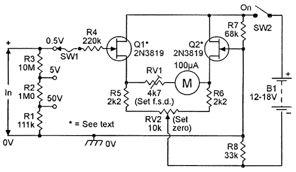
In practice, this very simple circuit tends to drift with variations in supply voltage and temperature, and fairly frequent trimming of the zero control is needed. Drift can be greatly reduced by using a zener-stabilized 12V supply.
Figure 15 shows an improved low-drift version of the JFET voltmeter. Q1 and Q2 are wired as a differential amplifier, so any drift occurring on one side of the circuit is automatically countered by a similar drift on the other side, and good stability is obtained. The circuit uses the ‘bridge’ principle, with Q1-R5 forming one side of the bridge and Q2-R6 forming the other. Q1 and Q2 should ideally be a matched pair of JFETs, with IDSS values matched within 10%. The circuit is set up in the same way as that of Figure 14.
MISCELLANEOUS JFET CIRCUITS
 |
| FIGURE 16. VLF astable multivibrator. |
 |
| FIGURE 17. Voltage-controlled amplifier/attenuator. |
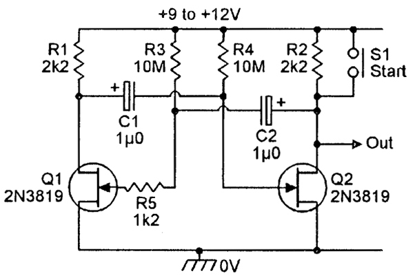
To conclude this month’s article, Figures 16 to 19 show a miscellaneous collection of useful JFET circuits. The Figure 16 design is that of a very-low-frequency (VLF) astable or free-running multivibrator; its on and off periods are controlled by C1-R4 and C2-R3, and R3 and R4 can have values up to 10M.
With the values shown, the circuit cycles at a rate of once per 20 seconds, i.e., at a frequency of 0.05Hz; start button S1 must be held closed for at least one second to initiate the astable action.
Figure 17 shows — in basic form — how a JFET and a 741 op-amp can be used to make a voltage-controlled amplifier/attenuator. The op-amp is used in the inverting mode, with its voltage gain set by the R2/R3 ratio, and R1 and the JFET are used as a voltage-controlled input attenuator.
When a large negative control voltage is fed to Q1 gate, the JFET acts like a near-infinite resistance and causes zero signal attenuation, so the circuit gives high overall gain but, when the gate bias is zero, the FET acts like a low resistance and causes heavy signal attenuation, so the circuit gives an overall signal loss.
Intermediate values of signal attenuation and overall gain or loss can be obtained by varying the control voltage value.
 |
| FIGURE 18. Constant-volume amplifier. |
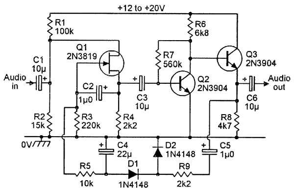
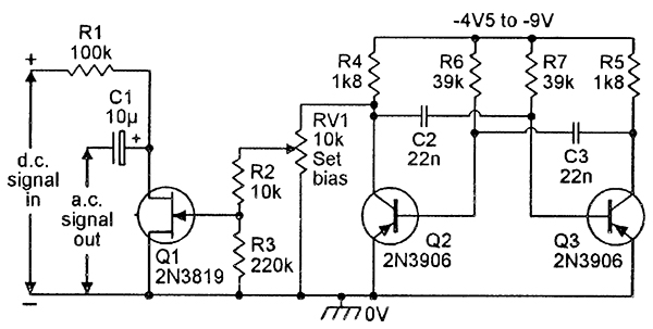
Figure 18 shows how this voltage-controlled attenuator technique can be used to make a ‘constant volume’ amplifier that produces an output signal level change of only 7.5dB when the input signal level is varied over a 40dB range (from 3mV to 300mV RMS).
The circuit can accept input signal levels up to a maximum of 500mV RMS Q1 and R4 are wired in series to form a voltage-controlled attenuator that controls the input signal level to common emitter amplifier Q2, which has its output buffered via emitter follower Q3.
Q3’s output is used to generate (via C5-R9-D1-D2-C4-R5) a DC control voltage that is fed back to Q1’s gate, thus forming a DC negative-feedback loop that automatically adjusts the overall voltage gain so that the output signal level tends to remain constant as the input signal level is varied, as follows.
When a very small input signal is applied to the circuit, Q3’s output signal is also small, so negligible DC control voltage is fed to Q1’s gate; Q1 thus acts as a low resistance under this condition, so almost the full input signal is applied to Q2 base, and the circuit gives high overall gain.
When a large input signal is applied to the circuit, Q3’s output signal tends to be large, so a large DC negative control voltage is fed to Q1’s gate; Q1 thus acts as a high resistance under this condition, so only a small part of the input signal is fed to Q2’s base, and the circuit gives low overall gain.
Thus, the output level stays fairly constant over a wide range of input signal levels; this characteristic is useful in cassette recorders, intercoms, and telephone amplifiers, etc.
 |
| FIGURE 19. DC-to-AC converter or ‘chopper’ circuit. |
Finally, Figure 19 shows a JFET used to make a DC-to-AC converter or ‘chopper’ that produces a squarewave output with a peak amplitude equal to that of the DC input voltage.
In this case, Q1 acts like an electronic switch that is wired in series with R1 and is gated on and off at a 1kHz rate via the Q2-Q3 astable circuit, thus giving the DC-to-AC conversion. Note that Q1’s gate-drive signal amplitude can be varied via RV1; if too large a drive is used, Q1’s gate-to-source junction starts to avalanche, causing a small spike voltage to break through the drain and give an output even when no DC input is present.
To prevent this, connect a DC input and then trim RV1 until the output is just on the verge of decreasing; once set up in this way, the circuit can be reliably used to chop voltages as small as a fraction of a millivolt. NV